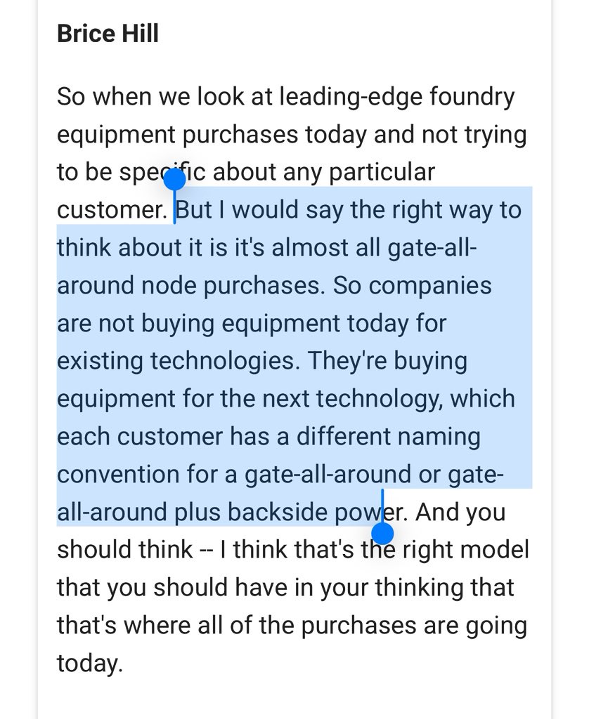
AMAT says almost all of leading edge purchases today are related to Gate-All-Around (GAA) or 2nm and below nodes. Sees 200 more steps for 2nm vs 3nm. 3nm has 1900 process steps, per AMAT. Also sees, HBM at 16% of DRAM wafer starts today (comments at BofA conference).
Source: Sravan Kundojjala
The copyright of this article belongs to the original author/organization.
The views expressed herein are solely those of the author and do not reflect the stance of the platform. The content is intended for investment reference purposes only and shall not be considered as investment advice. Please contact us if you have any questions or suggestions regarding the content services provided by the platform.


