How many wafers are needed per 1GW of computing power: Underlying calculation of AI equipment demand
Core Viewpoint
Over the past two years, market pricing for AI hardware has focused primarily on GPUs, HBM, and advanced packaging. As we enter 2026, industry constraints are shifting further upstream: the expansion of data center power capacity must ultimately translate into more GPU clusters, which consume not only advanced logic wafers but also simultaneously drive demand for HBM, server DRAM, and data center NAND.
Bernstein's baseline model shows that every additional 1GW of AI compute capacity requires approximately 46,000 wafers/month in new wafer fab capacity. If 50GW of AI capacity is added by 2030 compared to 2026, the corresponding incremental investment in wafer fab equipment would be approximately $376 billion. Adding this to the global semiconductor industry's existing expansion, equipment upgrades, and maintenance spending, global wafer fab equipment spending could reach $200 billion, $245 billion, and $291 billion in 2027, 2028, and 2029 respectively, totaling approximately $736 billion over the three years.
What makes this model truly noteworthy is not the single figure of $736 billion, but the shift in the structure of equipment spending: advanced logic is no longer the sole source of incremental demand; HBM, DRAM, and NAND combined may contribute about three-quarters of AI-related equipment investment.
I. 338GW Planned Capacity Does Not Directly Equate to Equipment Orders
As of June 2026, global operational data center capacity was approximately 50.7GW, an increase of about 11.4GW from a year ago; meanwhile, planned data center capacity expanded from approximately 121GW to 338GW, with new pipeline additions exceeding 200GW.
The growth rate of planned capacity far exceeds that of actual operational capacity, indicating that hyperscale cloud providers, Neoclouds, and data center operators are still accelerating the securing of land, power, and facility resources. However, 338GW is closer to a potential demand ceiling rather than deterministic compute delivery.
For a data center project to move from planning to operation, it must pass at least four constraints: grid connection, financing arrangements, chip delivery, and end-customer demand. Some projects have applied for land and power resources but have not yet signed long-term power purchase agreements; some facilities still lack clear GPU procurement plans; and some planned capacity may include duplicate applications and long-term reserve projects.
Therefore, one cannot simply multiply 338GW by the unit GW wafer demand to derive future equipment orders. Bernstein's baseline scenario is significantly lower than the total planned pipeline: assuming an addition of 50GW of AI capacity by 2030 compared to 2026, this equates to an average annual addition of approximately 12.5GW from 2027–2030, expanding AI data center capacity to approximately 3.5 times its 2026 level.
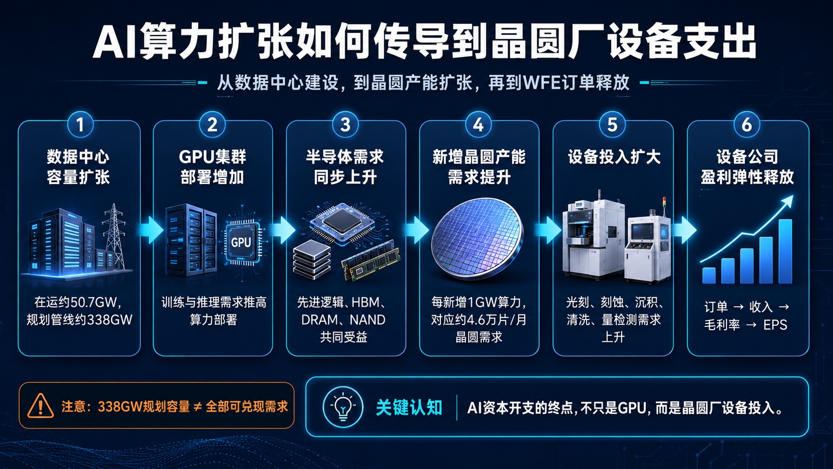
How AI Compute Expansion Transmits to Wafer Fab Equipment Spending: The complete path from data center capacity and GPU cluster deployment to wafer capacity and WFE orders.
II. Why Does Every Additional 1GW of Compute Require 46,000 Wafers/Month?
When discussing AI hardware, market attention usually centers on GPUs. However, an AI computing system consumes semiconductors far beyond just advanced logic chips.
GPUs handle the primary computation tasks, while CPUs and network chips manage system scheduling and interconnects. HBM handles high-bandwidth data exchange, traditional DRAM provides CPU-side memory, and NAND is used for storing model files, training data, checkpoints, and local caches. New compute capacity actually drives demand across all four categories: advanced logic, HBM, DRAM, and NAND.
Based on rack configurations at the Vera Rubin level, Bernstein calculates that every additional 1GW of AI compute capacity requires approximately 46,000 wafers/month in new wafer capacity, comprising approximately 25,000 wafers/month for DRAM, 9,000 for NAND, 8,000 for HBM, and 5,000 for advanced logic.
| Wafer Category | New Monthly Capacity per GW | Wafer Demand Share | Main Application |
|---|---|---|---|
| DRAM | Approx. 25,000 wafers | Approx. 54% | Server main memory and system cache |
| NAND | Approx. 9,000 wafers | Approx. 20% | Models, data, and local storage |
| HBM | Approx. 8,000 wafers | Approx. 17% | GPU high-bandwidth memory |
| Advanced Logic | Approx. 5,000 wafers | Approx. 11% | GPUs, CPUs, and network chips |
| Total | Approx. 46,000 wafers | Approx. 100% | — |
Key Insight
In terms of wafer volume, the largest incremental demand for AI infrastructure is not advanced logic, but memory. DRAM, HBM, and NAND combined account for nearly 90% of new wafer demand.
However, wafer volume does not directly equate to equipment revenue. The capital intensity per wafer for advanced logic fabs is significantly higher than for memory. Bernstein estimates that for every additional 10,000 wafers/month of capacity, advanced logic equipment investment is approximately $3.4 billion, HBM and DRAM approximately $1.4 billion, and NAND approximately $1.3 billion.
Thus, although advanced logic wafers represent a smaller share by volume, the value of lithography, deposition, etching, ion implantation, and metrology equipment is higher. Memory relies on larger wafer volumes, more stacking layers, and more complex process steps to generate equipment demand.
III. $376 Billion in Incremental Equipment Investment, Dominated by Memory
Under the scenario of 50GW of new AI capacity, Bernstein calculates related incremental wafer fab equipment investment at approximately $376 billion. This includes approximately $90 billion for advanced logic, $228 billion for HBM and DRAM, and $58 billion for NAND.
| Application Direction | Incremental Equipment Investment | Share |
|---|---|---|
| HBM and DRAM | Approx. $228 billion | Approx. 61% |
| Advanced Logic and Foundry | Approx. $90 billion | Approx. 24% |
| NAND | Approx. $58 billion | Approx. 15% |
| Total | Approx. $376 billion | 100% |
HBM, DRAM, and NAND combined contribute approximately 76% of incremental equipment investment. Therefore, the AI equipment cycle is not just a story of advanced logic and lithography; etching, deposition, thermal processing, cleaning, and process control equipment, which are memory-intensive, are also at the center of spending.
HBM is first and foremost an advanced DRAM front-end manufacturing business. Before forming stacked products, each layer of HBM requires independent DRAM wafer manufacturing, testing, and screening. As products evolve from 8-layer and 12-layer to 16-layer and higher, the number of bare dies required per sellable HBM continues to increase, leading to rising yield losses and redundant capacity needs.
DRAM demand comes from two paths. First, HBM occupies more advanced DRAM wafers, squeezing traditional server DRAM capacity. Second, AI servers themselves still require large-capacity CPU-side memory. With both types of demand growing simultaneously, memory manufacturers relying solely on product mix shifts cannot meet supply; net new wafer capacity becomes a more direct solution.
The equipment logic for NAND is easier to underestimate. Training and inference do not store all data in HBM; a vast amount of model files, vector databases, training data, and checkpoints still require local or near-line storage. As AI inference penetrates from the cloud to enterprise data centers, data center-level NAND demand may decouple from the traditional consumer electronics cycle.
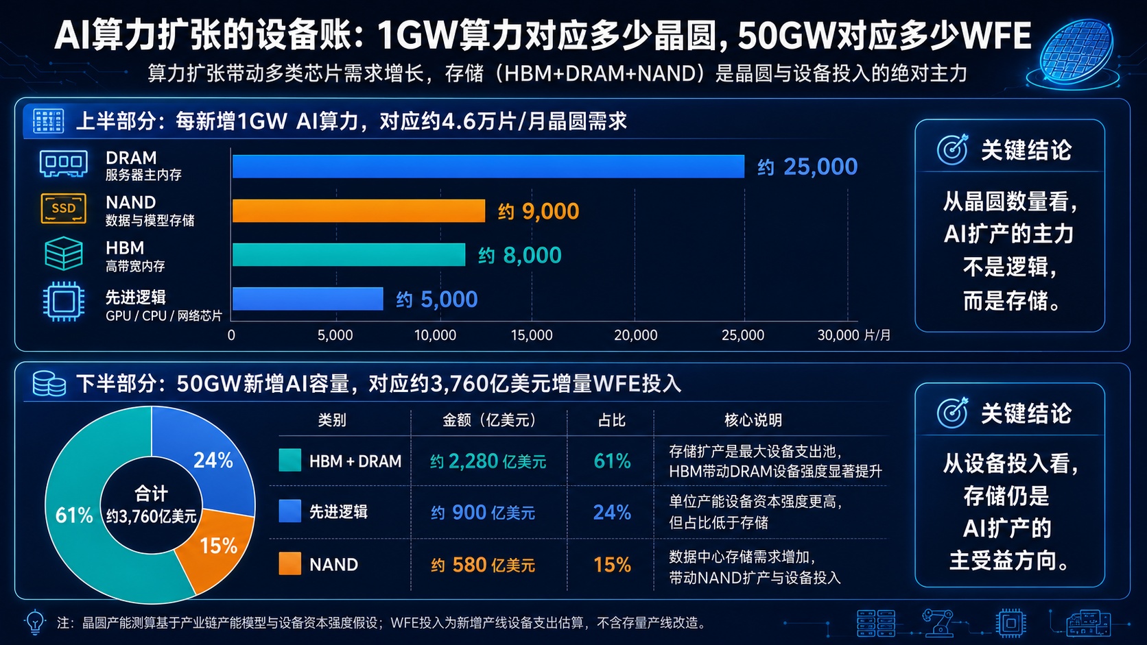
The structure of wafer demand corresponding to every additional 1GW of compute, and the distribution of approximately $376 billion in incremental equipment investment under the 50GW scenario.
IV. Why WFE May Approach $300 Billion from 2027–2029
AI-related incremental capacity is only part of global equipment spending. Wafer fabs also need to invest in mature processes, analog, power, automotive, and industrial chips, while maintaining upgrades, equipment replacements, and process migrations of existing lines.
Including these expenditures, Bernstein expects global WFE to rise from approximately $148 billion in 2026 to $200 billion in 2027, $245 billion in 2028, and $291 billion in 2029. The cumulative total for 2027–2029 will be approximately $736 billion, averaging about $245 billion annually.
| Year | Global WFE Scale | YoY Growth |
|---|---|---|
| 2025A | Approx. $122 billion | — |
| 2026E | Approx. $148 billion | Approx. 21% |
| 2027E | Approx. $200 billion | Approx. 35% |
| 2028E | Approx. $245 billion | Approx. 23% |
| 2029E | Approx. $291 billion | Approx. 19% |
The $736 billion cannot be entirely attributed to AI. A more accurate understanding is that AI demand may raise the global WFE center from the past range of $100–150 billion to $200–300 billion.
This differs from the traditional memory equipment cycle in two ways. First, the duration of demand may be longer. If equipment spending rises year-over-year from 2027–2029, the industry faces not a single peak year of expansion, but three consecutive years of capacity building. Second, the mid-cycle profit center may increase. If AI compute, memory, and storage demand keep WFE at a higher platform, the mid-cycle revenue, service revenue, and free cash flow of equipment companies will also shift upward accordingly.
The question is whether the market has already paid a high price for this scenario. Although major overseas equipment stocks have seen varying degrees of pullback from recent highs, their year-to-date gains and forward valuations remain at elevated levels. In the next phase, WFE upside can only provide a sector floor; it cannot guarantee excess returns for all equipment companies.
V. Etching and Deposition Are the First Priority for Memory Expansion
DRAM, HBM, and NAND are all etching and deposition-intensive products. High-layer NAND requires high aspect ratio etching within thick stacked structures; advanced DRAM requires constructing more complex capacitors, word lines, and contact holes; GAA transistors, backside power delivery, and novel interconnect structures will also add atomic layer deposition, selective etching, and new material processing steps.
Therefore, under the 50GW baseline scenario, Lam Research and Applied Materials have relatively high revenue sensitivity to new WFE. Lam's advantages lie in high aspect ratio etching and thin film deposition, making it more sensitive to capex changes in DRAM and NAND; Applied Materials has broader product coverage, offering a more balanced exposure between logic, memory, ion implantation, CMP, and advanced packaging.
Applied Materials reported Q1 FY2026 (ending April 2026) revenue of $7.91 billion, up 11% YoY; non-GAAP gross margin was 50.0%, and non-GAAP EPS was $2.86, up 20% YoY. The revenue growth rate is lower than the slope of Bernstein's WFE forecast for 2027–2029, meaning subsequent stock performance still depends on whether customer capex continues to be revised upward and whether the company can maintain its product share.
Lam Research's equipment structure is more skewed toward memory. If HBM, DRAM, and NAND become the main drivers of equipment investment, its earnings growth may outpace the industry; however, due to higher memory exposure, its earnings forecasts are also more susceptible to downward revisions if customers delay expansion.
VI. Metrology and Inspection Offer Smoother Revenue Elasticity and Higher Cash Flow Quality
While KLA's equipment volume may not grow linearly with wafer capacity like etching and deposition, the more complex the process, the higher the reliance of wafer fabs on defect detection, critical dimension metrology, and yield management.
The shift from FinFET to GAA in advanced logic, from single-layer DRAM to multi-layer stacking in HBM, and from traditional bumping to hybrid bonding in advanced packaging all increase defect costs. When failures are discovered in backend processes, the wafers, packaging, and testing costs already invested in the frontend may be completely lost; therefore, process control spending typically increases with the value per wafer.
KLA reported Q1 FY2026 (ending March 2026) revenue of $3.415 billion, GAAP diluted EPS of $9.12, and non-GAAP EPS of $9.40; quarterly free cash flow reached $622 million, with trailing twelve-month free cash flow of approximately $4.01 billion.
KLA's core advantage lies not in the volume surge of any single memory product, but in the simultaneous increase in process complexity across logic, memory, and advanced packaging. Even if final new data center capacity falls below the 50GW baseline, the process control intensity per wafer may still increase.
VII. ASML Provides Technological Monopoly, But Is Not the Highest Elasticity Asset in This Cycle
ASML remains an indispensable equipment supplier for advanced logic and advanced DRAM. Its core logic stems from increasing EUV penetration, the introduction of High-NA EUV, and the service and upgrade revenue generated by its massive installed base.
ASML reported Q2 2026 revenue of approximately €9.33 billion, with a gross margin of 54.0% and EPS of €7.59; the company raised its full-year revenue guidance to €43–45 billion, with gross margin guidance raised to 54–56%. Management also signaled that EUV capacity in 2027 is nearing full booking, with further expansion possible in 2028.
ASML's order visibility and technological barriers are at the highest level in the equipment industry, but its sensitivity to this round of AI incremental WFE is not the highest. This is because the largest expenditure pool in the 50GW model comes from HBM, DRAM, and NAND, while NAND has relatively limited dependence on EUV.
VIII. Overseas Equipment Stocks: Certainty and Elasticity Need Separate Pricing
| Company | Core Equipment | Main Beneficiary Direction | Earnings Attribute | Core Risk |
|---|---|---|---|---|
| ASML | EUV, DUV Lithography | Advanced Logic, Advanced DRAM | Monopolistic, High Order Visibility | Export Restrictions, Customer Expansion Pace |
| KLA | Inspection, Metrology, Process Control | Logic, HBM, Advanced Packaging | High Margin, High Cash Flow | High Valuation, Sector Spending Slowdown |
| Applied Materials | Deposition, Etching, Implantation, CMP | Logic, DRAM, NAND, Packaging | Platform-type, Balanced Exposure | Share Competition, Valuation Digestion |
| Lam Research | Etching, Deposition | DRAM, HBM, NAND | High Elasticity in Memory Cycle | Customer Capex Volatility |
If the investment goal is earnings certainty, ASML and KLA hold the advantage. If the goal is profit elasticity during the WFE upcycle, Lam Research is more direct. Applied Materials sits in between, benefiting from both advanced logic and memory expansion, as well as gaining incremental revenue from advanced packaging, CMP, and services.
IX. A-Share Equipment Chain Has Entered the Revenue Quality Verification Stage
Global WFE expansion provides a demand foundation for domestic equipment companies, but revenue growth for A-share equipment companies is also driven by domestic substitution, customer validation, and product share increases.
Compared to mature overseas equipment companies, domestic manufacturers are still in the product line expansion phase. From R&D, validation, bulk procurement to revenue recognition, new products go through a long cycle, accompanied by higher R&D, personnel, and supply chain investments. Revenue growth, non-GAAP profit, and operating cash flow may be significantly out of sync.
Naura Technology: Most Complete Platform Attributes, Profit Release is Key for Next Phase
Naura covers multiple equipment links including etching, thin film deposition, heat treatment, and cleaning, making it the semiconductor equipment company with the most complete product platform among A-shares.
In Q1 2026, the company's revenue was 10.323 billion yuan, up 25.80% YoY; net profit attributable to shareholders was 1.635 billion yuan, up 3.42% YoY; net operating cash flow was 748 million yuan. The revenue growth rate is significantly higher than the profit growth rate, indicating that R&D, personnel expansion, product structure, or expense inputs are still suppressing profit release.
Naura's core contradiction has shifted from "whether equipment can enter customer production lines" to "whether new products can form scale revenue and convert into profit and cash flow".
AMEC: Highest Match with Memory WFE Structure
AMEC's core asset is plasma etching equipment. Advanced logic, DRAM, HBM, and high-layer NAND all require higher aspect ratio, finer, and more selective etching processes.
In Q1 2026, AMEC's revenue was 2.915 billion yuan, up 34.13% YoY; net profit attributable to shareholders was 930 million yuan, up 197.20% YoY; non-GAAP net profit was 478 million yuan, up 60.09% YoY. The net profit includes investment income from equity sales, so the quality of main operations should be observed more through revenue, non-GAAP profit, and cash flow.
The upper limit of the company's subsequent valuation depends on two points: whether etching share can continue to increase, and whether thin film deposition and other new products can form a second revenue source.
TJX Technology: High Growth Slope, Low Valuation Error Tolerance
TJX Technology focuses on thin film deposition equipment such as PECVD, ALD, and SACVD, extending into equipment related to advanced processes, hybrid bonding, and 3D integration.
In Q1 2026, TJX's revenue was 1.112 billion yuan, up 56.97% YoY; net profit attributable to shareholders was 571 million yuan, non-GAAP net profit was 102 million yuan, and net operating cash flow was negative 520 million yuan. The significant difference between net profit and non-GAAP profit indicates that non-recurring items contributed significantly to current profits.
TJX has strong industrial logic, but the problem is that current pricing strictly demands order confirmation, acceptance progress, and profit margins.
Hwatsing Technology: Direct Mapping to Advanced Packaging, Relatively Balanced Risk-Reward Ratio
Hwatsing's core products include CMP, thinning, and wet chemical equipment. CMP benefits from increased interconnect layers in advanced logic, while thinning equipment directly maps to HBM stacking, Chiplet, and advanced packaging.
Compared to thin film deposition companies, Hwatsing's revenue slope may be smoother, but the market's pricing for future business is also relatively restrained. If thinning and other new products gradually form revenue, its valuation-growth match may be superior to equipment companies that have already priced in higher growth assumptions.
SAC Semiconductor: Stable Cleaning Base, New Equipment Determines Growth Slope
SAC Semiconductor centers on cleaning equipment, while expanding into electroplating, furnaces, photoresist coating/development, and advanced packaging equipment.
In Q1 2026, SAC's revenue was 1.476 billion yuan, up 13.06% YoY; net profit attributable to shareholders was 104 million yuan, down 57.66% YoY; non-GAAP net profit was 106 million yuan, down 57.24% YoY. The profit decline was mainly affected by exchange rates and financial expenses, but revenue growth was also lower than equipment companies like AMEC and TJX.
SAC's subsequent valuation space depends on whether electroplating, furnaces, photoresist coating/development, and advanced packaging equipment can form bulk revenue.
X. A-Share Equipment Stocks Cannot Be Ranked Solely by Revenue Growth
| Type | Representative Company | Core Logic | Main Verification Indicators |
|---|---|---|---|
| Platform Certainty | Naura Technology | Complete Product Line, Broad Customer Coverage | Gross Margin, Non-GAAP Profit, Operating Cash Flow |
| Memory Equipment Elasticity | AMEC, TJX Technology | Etching and Deposition Benefit from DRAM, HBM, NAND | New Product Revenue, Share, R&D Expense Ratio |
| Advanced Packaging and Process Upgrade | Hwatsing, SAC Semiconductor | CMP, Thinning, Cleaning, and Packaging Equipment | Order Structure, New Product Ramp-up, Receivables Collection |
For domestic equipment companies, four indicators are more important than revenue growth: whether non-GAAP net profit can approach revenue growth; whether contract liabilities and inventory structures are healthy; whether operating cash flow can improve alongside profits; and whether second and third product lines can form bulk revenue.
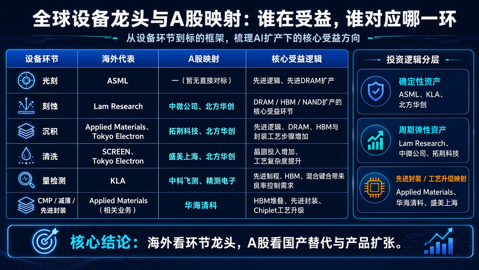
Mapping overseas leaders to A-share companies by equipment links: lithography, etching, deposition, cleaning, metrology/inspection, and CMP/thinning.
XI. Model Realization Still Subject to Three Constraints
1. Power Access May Become a Hard Constraint Earlier Than Chip Supply
50GW of new compute capacity requires long-term, stable, and low-cost power supply. Data centers that have already secured land may still face delays due to substation construction, transmission line approvals, and insufficient generation resources. If power access speed falls short of expectations, GPU deployment and wafer demand will both be pushed back.
2. Wafer Consumption per Unit of Compute May Decline
If unit chip performance grows faster than compute demand, the number of GPUs and memory required to achieve the same effective compute may decrease; conversely, if model parameters, inference calls, and context lengths continue to grow, wafer demand may exceed current estimates. The 46,000 wafers/month per GW figure is better suited as an industry estimation framework rather than a fixed constant.
3. Reuse of Existing Equipment May Reduce New Procurement Amounts
Memory manufacturers do not necessarily rely entirely on new wafer fabs to meet demand. Process migration, equipment upgrades, product mix adjustments, and yield improvements can all increase the effective output of existing lines. If the degree of reuse of existing equipment is higher than expected, new equipment procurement will be lower than the model predicts.
XII. Buyer Conclusion: Industry Still Expanding, But Equipment Stocks Have Entered the Realization Phase
AI infrastructure investment is spreading from GPU procurement to wafer manufacturing capabilities. Every additional 1GW of compute requires not only advanced logic chips but also larger-scale HBM, server DRAM, and data center NAND. The resulting wafer demand is driving the semiconductor equipment industry from a single advanced logic cycle to a synchronized expansion of logic and memory.
Bernstein's calculated $736 billion WFE for 2027–2029 is not a deterministic outcome, but its direction of spending possesses industrial rationality. Even if the 50GW baseline scenario is only partially realized, the global WFE center may still remain higher than past cycles. What needs to be wary of now is not a sudden disappearance of industry demand, but the fact that equipment stocks have already priced in strong growth expectations for 2027–2029.
Among overseas equipment stocks, ASML and KLA's core value lies in technological barriers, order visibility, and cash flow quality; Lam Research is a high-elasticity asset for the rebound in memory capex; Applied Materials provides comprehensive exposure to logic, memory, and advanced packaging.
In the A-share equipment chain, Naura remains the core platform asset, but needs profit margins and cash flow to realign with revenue growth; AMEC has the highest fit with memory equipment spending structure; TJX Technology has a high growth slope, but current pricing strictly demands performance realization; Hwatsing has a relatively balanced risk-reward ratio in CMP, thinning, and advanced packaging; SAC Semiconductor needs to improve its growth slope through equipment beyond cleaning.
Investment Framework
Excess returns for equipment stocks in the next phase will not come from the consensus of "AI capex growth" itself, but from three more specific variables: who occupies the fastest-growing process segments in equipment spending, who can increase share during customer expansion, and who can convert orders into non-GAAP profit and free cash flow.
Risk Warning
The industry calculations involved in this article rely on assumptions regarding new data center capacity, rack configurations, wafer consumption, equipment capital intensity, and wafer fab expansion pace. Actual results may be affected by power access, capex adjustments, chip architecture changes, yield improvements, equipment reuse, export restrictions, and macroeconomic cycles. The companies and data mentioned in this article are for industrial research purposes only and do not constitute any investment advice.
The copyright of this article belongs to the original author/organization.
The views expressed herein are solely those of the author and do not reflect the stance of the platform. The content is intended for investment reference purposes only and shall not be considered as investment advice. Please contact us if you have any questions or suggestions regarding the content services provided by the platform.