 07709 Return Rate
High integration is an inevitable trend in the chip industry. Advanced packaging is the "super glue + Lego bricks" to realize this trend. The explosion of AI computing power has turned it from a "supporting role" to a "leading role," with growth far exceeding the semiconductor industry average.
1. What is advanced packaging? First, understand what "packaging" does. A chip can be imagined as: Bare Die: The thin silicon wafer with transistors etched on it, the "brain" of the chip. Packaging: The "protective clothing + connecting wires" for the brain, responsible for three things: protecting the silicon from physical damage, moisture, and static electricity; leading out the chip's signals and power to communicate with the motherboard; and helping the chip dissipate heat to avoid burning out. Traditional packaging: Like putting a large CPU in a separate box and connecting it to the motherboard with long wires — signals travel far, resulting in slow speed, high power consumption, and taking up space. Advanced packaging: Like tightly integrating "small chips" (Chiplets) like CPU, GPU, and memory using "nano-scale highways" (high-density interconnects). Some are side-by-side (2.5D/CoWoS), some are stacked vertically (3D packaging), equivalent to condensing an entire computer host into a small cube.
2. Why has advanced packaging suddenly "caught fire"? Three core drivers: 1. Moore's Law is "slowing down," advanced packaging becomes the "lifesaver." Previously, chip performance improvement relied on "shrinking transistors" (e.g., from 14nm to 3nm). But now: Physical limits: Transistors are approaching atomic sizes; any smaller leads to leakage and instability. Cost explosion: Costs double for processes below 7nm; a 3nm production line costs $50 billion, affordable only to a few giants. Advanced packaging takes a different approach: not pursuing smaller individual chips, but "stitching" multiple chips more tightly, trading "integration density" for performance, with lower costs and higher flexibility. 2. AI computing power demand is "skyrocketing," making advanced packaging a "necessity." Large model training requires trillions of calculations per second, with data frantically transmitted between CPU, GPU, and memory. The "long wires" of traditional packaging become a bottleneck: data travels too slowly and wastes electricity. Advanced packaging solutions: CoWoS+ HBM: Placing GPU and high-bandwidth memory (HBM) side-by-side, connected by countless "nano-wires," increasing data transfer speed by 10x and reducing power consumption by 50%. — AI flagship chips like NVIDIA H100/B200 and AMD MI300 rely entirely on this. Chiplet: Breaking a large chip into multiple small chips (e.g., compute chiplets, memory chiplets) and combining them like building blocks. If one fails, it can be replaced, reducing R&D costs by 30-50%. 3. End devices are "getting smaller," requiring "higher and higher" integration. Phones need to be thin and light yet powerful; cars need to fit dozens of chips without taking up space; VR/AR glasses have even less room. Advanced packaging can "compress" multiple chips with different functions to 1/10 of their original volume without compromising performance.

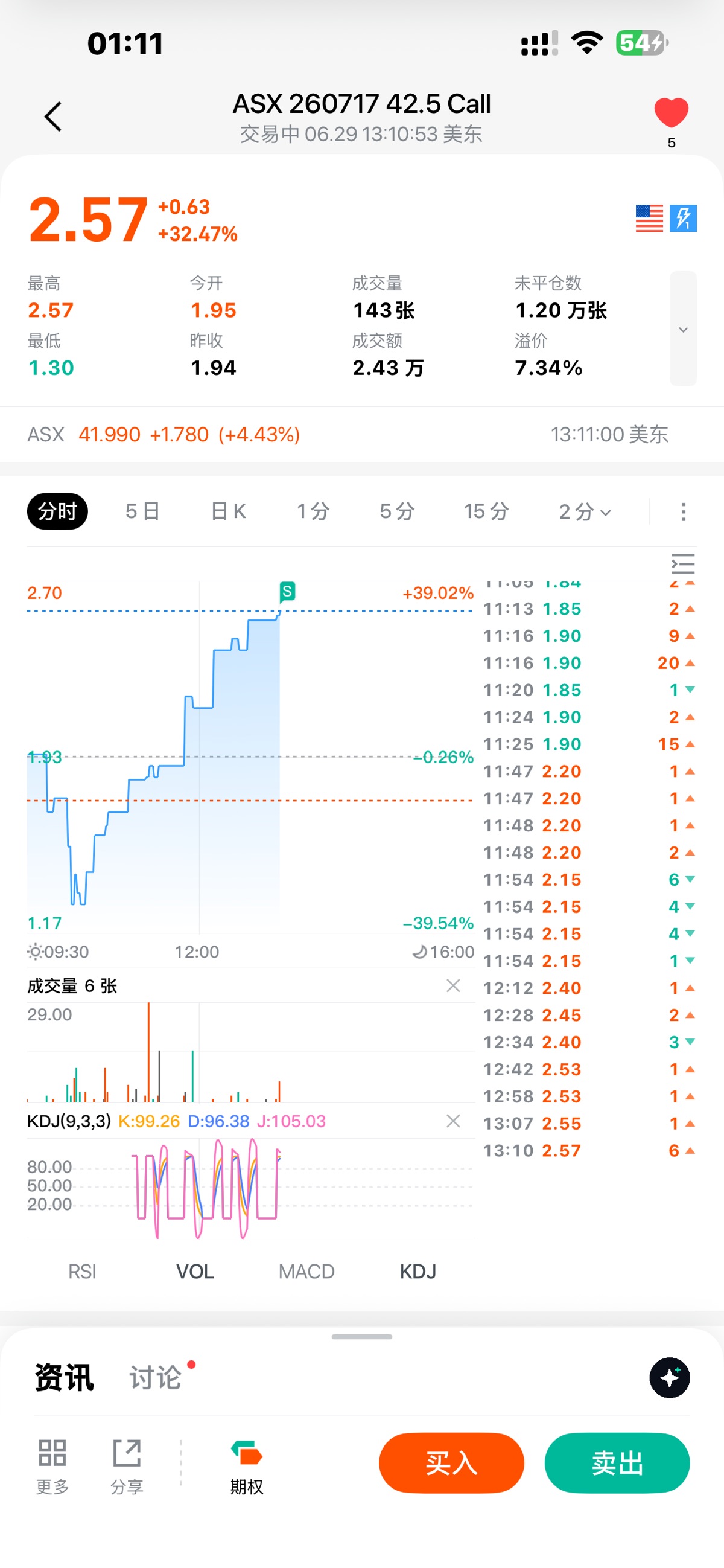
$Advanced Semiconductor Engineering(ASX.US)
Don't feel inferior and anxious because of your own laziness.
If you become diligent, you might end up causing even bigger trouble🌝🤔
Night🥸
The copyright of this article belongs to the original author/organization.
The views expressed herein are solely those of the author and do not reflect the stance of the platform. The content is intended for investment reference purposes only and shall not be considered as investment advice. Please contact us if you have any questions or suggestions regarding the content services provided by the platform.